
Event Description
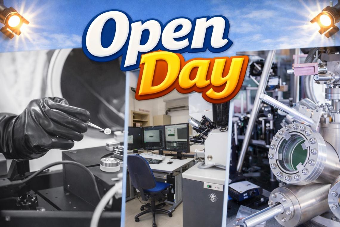
The ALL-MICRO Open Day offers a unique opportunity for companies, industries, hospitals, and medical centers to explore advanced research infrastructure, cutting-edge microscopy technologies, and innovative scientific activities.
Participants will have the chance to visit specialized laboratories, engage with experts, and discover how these technologies can be applied across different sectors.
Program
Morning Session (10:00)
- 10:00 – Welcome and presentation of the ALL-MICRO network
- 10:15 – Visit: Focus Ion Beam (FIB)
- 10:45 – Visit: Advanced Quantum Devices Laboratory
- 11:15 – Visit: 4-Probe STM microscopy
- 11:45 – Q&A
Afternoon Session (13:00)
- 13:00 – Welcome and presentation of the ALL-MICRO network
- 13:15 – Visit: Focus Ion Beam (FIB)
- 13:45 – Visit: Advanced Quantum Devices Laboratory
- 14:15 – Visit: 4-Probe STM microscopy
- 14:45 – Q&A
Important Information
- The program lasts approximately 2 hours and is identical for both sessions
- Each laboratory visit lasts 30 minutes
- Maximum number of participants per laboratory: 5 persons
Registration
To participate, please fill out the application form (linked below) and send it to:
info@nanocenter.si
The application form requires the following information:
- Name and surname
- Position
- Email and phone number
- Institution/company name and address
Limited Availability
Places are limited, so early registration is strongly recommended.
___________________________________________________________________________________________
Focused Ion Beam (FIB) is a highly advanced scientific instrument that functions as both a processing tool and an electron microscope in one. Originally developed for the semiconductor industry, a FIB system typically consists of two separate columns: The Electron Column: Primarily used for high-resolution imaging of samples. The Ion Column: Enables etching, nanostructuring, and various other investigations across a wide range of materials.
In collaboration with industry, the FIB has proven to be an indispensable instrument for: Determining the structure of coatings and thin films, Analyzing alloys and microstructures., Conducting defect studies and quality control., Researching material homogeneity.
The instrument is utilized for creating complex shapes and patterns at the nanometer scale, as well as for: TEM Sample Preparation: Creating ultra-thin cross-sections for Transmission Electron Microscopy., 3D Tomography: Serial sectioning to reconstruct three-dimensional internal structures., Ion Beam Induced Deposition (IBID): Applying conductive or non-conductive thin layers using the ion beam and more.
Advanced Quantum Devices Laboratory – AQDL is a new nanofabrication, test and measurement facility dedicated to serving a wide community of academia and industry. The facility includes an anaerobic environment for nanolithography and device fabrication, exfoliated monolayer crystal positioning, patterning and transport measurements over a large range of temperatures, and up to 2.5T magnetic field. Its operation is integrated with access to state of the art European nanofabrication facilities.
The 4-probe STM UHV system is a powerful microscopy system designed for characterization and processing of thin films and nanostructures. Microscope stage combines 4 probes that act as tips for atomic resolution scanning tunnelling microscopy and one of them can also perform atomic force microscopy. To facilitate better control and positioning over probes and the sample and to perform basic electron microscopy, a scanning electron microscope is installed above the chamber. The system enables precise 4-point measurements of electronic transport and nanostructure manipulation.
| Mon | Tue | Wed | Thu | Fri | Sat | Sun |
|---|---|---|---|---|---|---|
|
|
|
|
||||
|
|
|
|
|
|
||
|
|
|
|
|
|
|
|
|
|
|
|
|
|
|
|
|
|
|
|
|
|
|
|